

A high school student in his curriculum; will come across certain electronics and electrical experiments. One of them related to semiconductor devices such as Bipolar Junction Transistors (BJTs) and Field Effect Transistors (FETs). PSLab device is capable of function as a waveform generator, voltage and current source, oscilloscope and multimeter. Using these functionalities one can design an experiment. This blog post brings out the basics one should know about the experiment and the PSLab device to program an experiment in the saved experiments section.
Channels and Sources in the PSLab Device
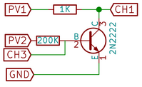
Programmable Voltage Sources can generate voltages as follows;
- PV1 → -5V ~ +5V
- PV2 → -3.3V ~ +3.3V
- PV3 → 0 ~ +3.3V
Programmable Current Source (PCS) can generate current as follows;
- PCS → 0 ~ 3.3mA
The device has 4 channel oscilloscope out of those CH1, CH2 and CH3 pins are useful in experiments of the current context type.
About BJTs and FETs
Every semiconductor device is made of Silicon(Si). Some are made of Germanium(Ge) but they are not widely used. Silicon material has a potential barrier of 0.7 V among P type and N type sections of a semiconductor device. This voltage value is really important in an experiment as in some practicals such as “BJT Amplifier”, there is no use of a voltage value setting below this value. So the experiment needs to be programmed to have 0.7V as the minimum voltage for Base terminal.
Basic BJT experiments
BJTs have three pins. Collector, Emitter and Base. Current to the Base pin will control the flow of electrons from Emitter to Collector creating a voltage difference between Collector and Emitter pins. This scenario can be taken down to three types as;
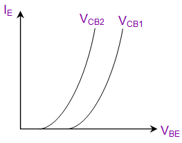
- Input Characteristics → Relationship between Emitter current to VBE(Base to Emitter)
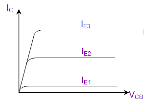
- Output Characteristics → Relationship between IC(Collector) to VCB(Collector to Base)
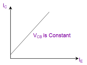
- Transfer Characteristics → Relationship between IC(Collector) to IE(Emitter)
|
Input Characteristics |
Output Characteristics |
Transfer Characteristics |
 |
 |
 |
Basic FET experiments
FETs have three pins. Drain, Source and Gate. Voltage to Gate terminal will control the electron flow from either direction from or to Source and Drain. This scenario results in two types of experiments;
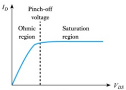
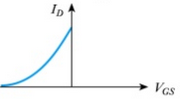
- Output Characteristics → Drain current to Drain to Source voltage difference
- Transfer Characteristics → Gate to Source voltage to Drain current
| Output Characteristics | Transfer Characteristics |
 |
 |
Using existing methods in PSLab android repository
Current implementation of the android application consists of all the methods required to read voltages and currents from the relevant pins and fetch waveforms from the channel pins and output voltages from PVS pins.
ScienceLab.java class – This class implements all the methods required for any kind of an experiment. The methods that will be useful in designing BJT and FET related experiments are;
Set Voltages
public void setPV1(float value);
public void setPV2(float value);
public void setPV3(float value);
Set Currents
public void setPCS(float value);
Read Voltages
public double getVoltage(String channelName, Integer sample);
Read Currents
To read current there is no direct way implemented. The current flow between two nodes can be calculated using the PVS pin value and the voltage value read from the channel pins. It uses Ohm’s law to calculate the value using the known resistance between two nodes.
IC = (PV1 – CH1) / 1000
This is how it is actually implemented in the existing experiments.
If one needs to implement a new experiment of any kind, these are the basics need to know. There can be so many new experiments implemented using these basics. Some of them could be;
- Effect of Temperature coefficient in Collector current
- The influence in β factor in Collector current
Resources:
- Experiments Section in Android Repo: https://github.com/fossasia/pslab-android/tree/master/app/src/main/java/org/fossasia/pslab/experimentsetup
- BJT Characteristics: http://fourier.eng.hmc.edu/e84/lectures/ch4/node3.html
- FET Characteristics: https://electronicspost.com/describe-the-output-characteristics-and-transfer-characteristics-of-jfet-explain-different-methods-of-biasing-of-a-jfet/