How to get a cost effective PCB for Production

Designing a PCB for a DIY project involves in making up the schematics which then turned into a PCB layout. Components used in these PCBs will be mostly “Through Hole” which are commonly available in the market. Once the PCB is printed in either screen printing techniques or using photo resistive dry films, making alterations to the component mounting pads and connections will be somewhat possible. When dealing with a professional PCB design, there are many properties we need to consider. DIY PCBs will simply be single sided in most cases. A professional printed circuit board will most likely to have more than one layer. The PCB for PSLab device has 4 layers. Adding more layers to a PCB design makes it easier to draw connections. But on the other hand, the cost will increase exponentially. The designer must try to optimize the design to have less layers as much as possible. The following table shows the estimated cost for printing for 10 PSLab devices if the device had that many layers. One Layer Two Layers Four Layers Six Layers $4.90 $4.90 $49.90 $305.92 Once the layer levels increase from 2, the other layers will be inner layers. The effective area of inner layers will be reduced if the designer adds more through hole components or vias which connects a connection from a one layer with a connection with another layer. The components used will then be limited to surface mount components. Surface Mount components (SMD) are expensive compared to their Through Hole (TH) counterpart. But the smaller size of SMD makes it easier to place many components in a smaller area than to Through Hole components. Soldering and assembling Through Hole components can be done manually using hand soldering techniques. SMD components need special tools and soldering equipments to assemble and solder them. Much more precision is required when SMD components are soldered. Hence automated assembly is used in industry where robot arms are used to place components and reflow soldering techniques to solder the SMD components. This emphasizes that the number of SMD components used in the PCB will increase the assembly cost as well as the component cost but it will greatly reduce the size of the PCB. SMD components comes in different packages. Passive components such as resistors, capacitors will come in 0.25 mm upto 7.4mm dimensions. PSLab device uses 0805/2012 sized package which is easier to find in the market and big enough to pick and assemble by hand. The packaging refers to its dimensions. 0805 reads as 0.08 inches long and 0.05 inches wide. Finding the components in the market is the next challenging task. We can easily purchase components from an online store but the price will be pretty high. If the design can spare some space, it will be wise to have alternative pads for a Through Hole component for the SMD component as Through Hole components can be found much easier than SMD components in a local store. The following image…

Continue ReadingHow to get a cost effective PCB for Production

Creating Bill of Materials for PSLab using KiCAD

PSLab device consists of a hundreds of electronic components. Resistors, diodes, transistors, integrated circuits are to name a few. These components are of two types; Through hole and surface mounted. Surface mount components (SMD) are smaller in size. Due to this reason, it is hard to hand solder these components onto a printed circuit board. We use wave soldering or reflow soldering to connect them with a circuit. Through Hole components (TH) are fairly larger than their SMD counter part. They are made bigger to make it easy for hand soldering. These components can also be soldered using wave soldering. Once a PCB has completed its design, the next step is to manufacture it with the help of a PCB manufacturer. They will require the circuit design in “gerber” format along with its Bill of Materials (BoM) for assembly. The common requirement of BoM is the file in a csv format. Some manufacturers will require the file in xml format. There are many plugins available in KiCAD which does the job. KiCAD when first installed, doesn’t come configured with a BoM generation tool. But there are many scripts developed with python available online free of charge. KiBoM is one of the famous plugins available for the task. 
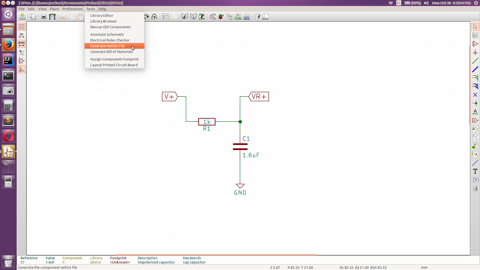
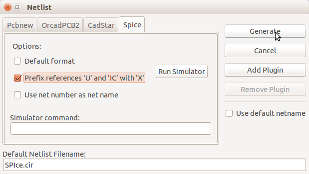
Go to “Eeschema” editor in KiCAD where the schematic is present and then click on the “BoM” icon in the menu bar. This will open a dialog box to select which plugin to use to generate the bill of materials. Initially there won’t be any plugins available in the “Plugins” section. As we are adding plugins to it, they will be listed down so that we can select which plugin we need. To add a plugin, click on the “Add Plugin” button to open the dialog box to browse to the specific plugin we have already downloaded. There are a set of available plugins in the KiCAD installation directory. The path is most probably will be (unless you have made any changes to the installation); usr/lib/kicad/plugins Once a plugin is selected, click on “Generate” button to generate the bom file. “Plugin Info” will display where the file was made and it’s name. Make sure we have made the BoM file compatible to the file required by the manufacturer. That is; removed all the extra content and added necessary details such as manufacturer’s part numbers and references replacing the auto generated part numbers. Resources: Through Hole : https://en.wikipedia.org/wiki/Through-hole_technology Surface Mount : https://en.wikipedia.org/wiki/Surface-mount_technology Wave Soldering : https://en.wikipedia.org/wiki/Wave_soldering Reflow Soldering : https://en.wikipedia.org/wiki/Reflow_soldering Gerber Format : https://en.wikipedia.org/wiki/Gerber_format KiCAD BoM Library : https://github.com/SchrodingersGat/KiBoM

Continue ReadingCreating Bill of Materials for PSLab using KiCAD

KiCAD Simulation to Validate Circuitry in PSLab Device

A circuit is a combination of passive or active electronic components which are interconnected with wires and provided to power to perform a specific task. Bringing a conceptual circuit design into an actual model includes several steps. It all starts with a problem definition such as a “Power module to regulate input voltage to output 5V”. The next step is to design the schematic with the help of a designing tool. Once the schematic is complete, the PCB layout can be made which will be later printed out as the final circuit. The importance of testing the schematic circuit for performance and functionalities is very important as once the circuit is printed out, there is no way to modify the wiring or components. That is when the SPICE simulation comes into picture. PSLab device is consisted of hundreds of circuit components and they are interconnected using a 4 layer printed circuit board. A fault in one sub circuitry may fail the complete device. Hence each of them must be tested and simulated using proper tools to ensure functionality against a test input data set. KiCAD requires an external SPICE engine to be installed. Ngspice is a famous SPICE tool used in the industry. The test procedures carried out to ensure the circuitry functions in PSLab device is described in this blog. Once the circuit is complete, generate the spice netlist. This will open up a dialog box and in the “Spice” tab, select “Prefix references ‘U’ and ‘IC’ with ‘X’”. U and IC prefixes are used with chips which cannot be simulated with SPICE. Click “Generate” to build the netlist. Note that this is not the netlist we use to build up the PCB but a netlist which can be used in SPICE simulation. Now browse to the project folder and rename the file extension of cir to cki to make them compatible with command line SPICE commands. cp <filename>.cir <filename>.cki Then open the file using a text editor and modify the GND connection to have a global ground connection by replacing “GND” with “0” which is required in SPICE simulation. Once the SPICE code is complete run the following commands to get the SPICE script compiled; export SPICE_ASCIIRAWFILE=1 ngspice -b -r <filename>.raw <filename>.cki ngnutmeg SPIce.raw This will open up a data analysis and manipulation program provided with ngspice to plot graphs and analyse SPICE simulations. Using this we can verify if the circuit can produce expected outputs with respect to the inputs we are providing and make adjustments if necessary. Resource: Ngspice: http://ngspice.sourceforge.net/download.html Installing ngspice: http://web.engr.oregonstate.edu/~traylor/ece 391/install_ngspice Sample SPICE simulations: https://www.allaboutcircuits.com/text book/reference/chpt-7/example-circuits-and-netlists/ SPICE Commands and syntaxes: http://www.ecircuitcenter.com/ SPICEsummary.htm PSLab Hardware repository: https://github.com/fossasia/ pslab-hardware/

Continue ReadingKiCAD Simulation to Validate Circuitry in PSLab Device

Controlling Motors using PSLab Device

PSLab device is capable of building up a complete science lab almost anywhere. While the privilege is mostly taken by high school students and teachers to perform scientific experiments, electronic hobbyists can greatly be influenced from the device. One of the usages is to test and debug sensors and other electronic components before actually using them in their projects. In this blog it will be explained how hobbyist motors are made functional with the use of the PSLab device. There are four types of motors generally used by hobbyists in their DIY(Do-It-Yourself) projects. They are; DC Gear Motor DC Brushless Motor Servo Motor Stepper Motor DC motors do not require much of a control as their internal structure is simply a magnet and a shaft which was made rotatable around the magnetic field. The following image from slideshare illustrates the cross section of a motor. These motors require high currents and PSLab device as it is powered from a USB port from a PC or a mobile phone, cannot provide such high current. Hence these type of motors are not recommended to use with the device as there is a very high probability it might burn something. 
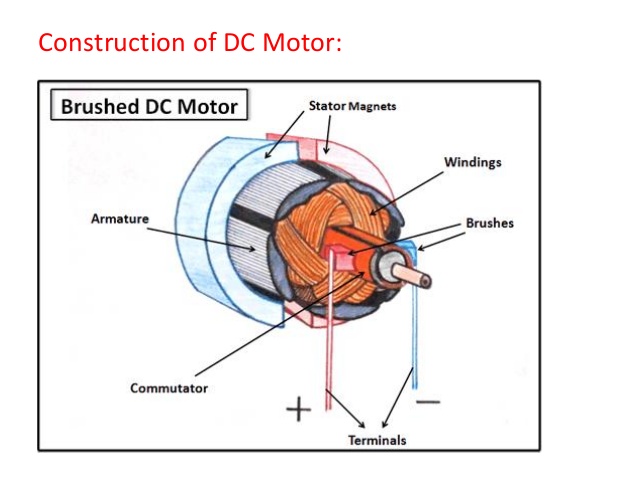
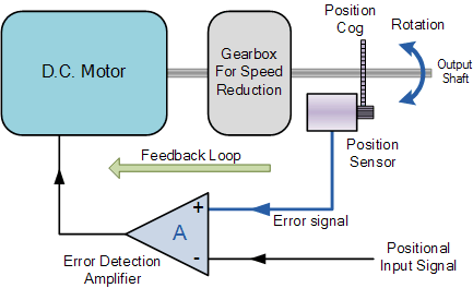
In the current context, we are concerned about stepper motors and servo motors. They cannot be powered up using direct currents to them. Inside these motors, the structure is different and they require a set of controlled signals to function. The following diagram from electronics-tutorials illustrates the feedback loop inside a servo motor. A servo motor is functional using a PWM wave. Depending on the duty cycle, the rotational angle will be determined. PSLab device is capable of generating four different square waves at any duty cycle varying from 0% to 100%. This gives us freedom to acquire any angle we desire from a servo motor. The experiment “Servo Motors” implement the following method where it accepts four angles. public void servo4(double angle1, double angle2, double angle3, double angle4) The experiment supports control of four different servo motors at independant angles. Most of the servos available in the market support only 180 degree rotation where some servos can rotate indefinitely. In such a case, the servo will rotate one cycle and reach its initial position. 
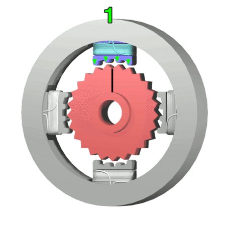
The last type of motor is stepper motor. As the name says it, this motor can produce steps. Inside of the motor, there are four coils and and five wires coming out of the motor body connecting these coils. The illustration from Wikipedia shows how four steps are acquired by powering up the respective coil in order. This powering up process needs to be controlled and hard to do manually. Using PSLab device experiment “Stepper Motor”, a user can acquire any number of steps just by entering the step value in the text box. The implementation consists of a set of method calls; scienceLab.stepForward(steps, 100); scienceLab.stepBackward(steps, 100); A delay of 100 milliseconds is provided so that there is enough time to produce a step. Otherwise the shaft will…

Continue ReadingControlling Motors using PSLab Device

Basics behind school level experiments with PSLab

Electronics is a fascinating subject to most kids. Turning on a LED bulb, making a simple circuit will make them dive into much more interesting areas in the field of electronics. PSLab android application with the help of PSLab device implements a set of experiments whose target audience is school children. To make them more interested in science and electronics, there are several experiments implemented such as measuring body resistance, lemon cell experiment etc. This blog post brings out the basics in implementing these type of experiments and pre-requisite. Lemon Cell Experiment 
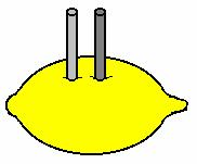
Lemon Cell experiment is a basic experiment which will make school kids interested in science experiments. The setup requires a fresh lemon and a pair of nails which is used to drive into the lemon as illustrated in the figure. The implementation in PSLab android application uses it’s Channel 1. The cell generates a low voltage which can be detected using the CH1 pin of PSLab device and it is sampled at a rate of 10 to read an accurate result. float voltage = (float) scienceLab.getVoltage("CH1", 10); 2000 instances are recorded using this method and plotted against each instance. The output graph will show a decaying graph of voltage measured between the nails driven into the lemon. for (int i = 0; i < timeAxis.size(); i++) { temp.add(new Entry(timeAxis.get(i), voltageAxis.get(i))); } Human Body Resistance Measurement Experiment 
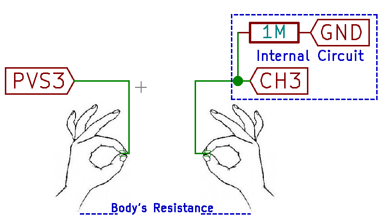
This experiment attracts most of the young people to do electronic experiments. This is implemented in the PSLab android application using Channel 3 and the Programmable Voltage Source 3 which can generate voltage up to 3.3V. The experiment requires a human with drippy palms so it makes a good conductance between device connection and the body itself.
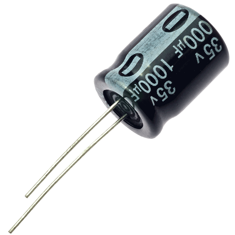
 The PSLab device has an internal resistance of 1M Ohms connected with the Channel 3 pin. Experiment requires a student to hold two wires with the metal core exposed; in both hands. One wire is connected to PV3 pin when the other wire is connected to CH3 pin. When a low voltage is supplied from the PV3 pin, due to heavy resistance in body and the PSLab device, a small current in the range of nano amperes will flow through body. Using the reading from CH3 pin and the following calculation, body resistance can be measured. voltage = (float) scienceLab.getVoltage("CH3", 100); current = voltage / M; resistance = (M * (PV3Voltage - voltage)) / voltage; This operation is executed inside a while loop to provide user with a continuous set of readings. Using Java threads there is a workaround to implement the functionalities inside the while loop without overwhelming the system. First step is to create a object without any attribute. private final Object lock = new Object(); Java threads use synchronized methods where other threads won’t start until the first thread is completed or paused operation. We make use of that technique to provide enough time to read CH3 pin and display output. while (true) { new MeasureResistance().execute(); synchronized (lock) { try { lock.wait();…

Continue ReadingBasics behind school level experiments with PSLab

Basics behind BJT and FET experiments in PSLab

A high school student in his curriculum; will come across certain electronics and electrical experiments. One of them related to semiconductor devices such as Bipolar Junction Transistors (BJTs) and Field Effect Transistors (FETs). PSLab device is capable of function as a waveform generator, voltage and current source, oscilloscope and multimeter. Using these functionalities one can design an experiment. This blog post brings out the basics one should know about the experiment and the PSLab device to program an experiment in the saved experiments section. Channels and Sources in the PSLab Device 
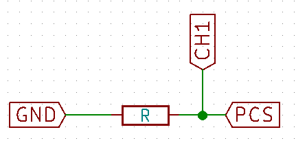
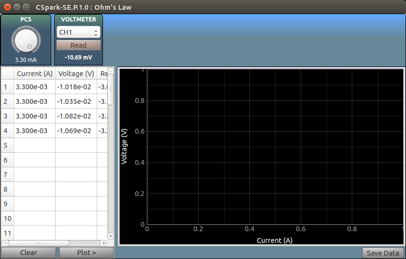
The PSLab device has three pins dedicated to function as programmable voltage sources (PVS) and one pin for programmable current source (PCS).
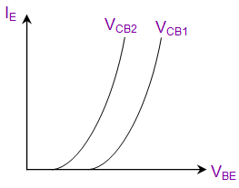
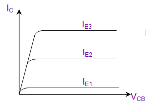
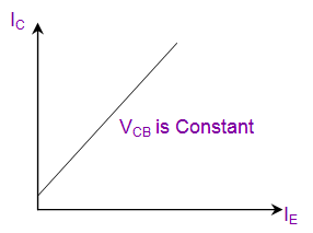
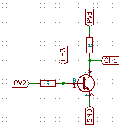
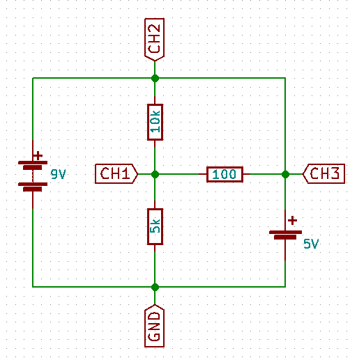
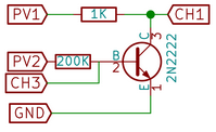
 Programmable Voltage Sources can generate voltages as follows; PV1 →  -5V ~ +5V PV2 → -3.3V ~ +3.3V PV3 → 0 ~ +3.3V Programmable Current Source (PCS) can generate current as follows; PCS → 0 ~ 3.3mA The device has 4 channel oscilloscope out of those CH1, CH2 and CH3 pins are useful in experiments of the current context type. About BJTs and FETs Every semiconductor device is made of Silicon(Si). Some are made of Germanium(Ge) but they are not widely used. Silicon material has a potential barrier of 0.7 V among P type and N type sections of a semiconductor device. This voltage value is really important in an experiment as in some practicals such as “BJT Amplifier”, there is no use of a voltage value setting below this value. So the experiment needs to be programmed to have 0.7V as the minimum voltage for Base terminal. Basic BJT experiments BJTs have three pins. Collector, Emitter and Base. Current to the Base pin will control the flow of electrons from Emitter to Collector creating a voltage difference between Collector and Emitter pins. This scenario can be taken down to three types as; Input Characteristics → Relationship between Emitter current to VBE(Base to Emitter) Output Characteristics → Relationship between IC(Collector) to VCB(Collector to Base) Transfer Characteristics → Relationship between IC(Collector) to IE(Emitter) Input Characteristics Output Characteristics Transfer Characteristics       Basic FET experiments FETs have three pins. Drain, Source and Gate. Voltage to Gate terminal will control the electron flow from either direction from or to Source and Drain. This scenario results in two types of experiments; Output Characteristics → Drain current to Drain to Source voltage difference Transfer Characteristics → Gate to Source voltage to Drain current Output Characteristics Transfer Characteristics Using existing methods in PSLab android repository Current implementation of the android application consists of all the methods required to read voltages and currents from the relevant pins and fetch waveforms from the channel pins and output voltages from PVS pins. ScienceLab.java class - This class implements all the methods required for any kind of an experiment. The methods that will be useful in designing BJT and FET related experiments are; Set Voltages public void setPV1(float value); public void setPV2(float value); public void setPV3(float value); Set Currents public void setPCS(float value); Read Voltages public…

Continue ReadingBasics behind BJT and FET experiments in PSLab

Implementing Experiment Functionality in PSLab Android

Using the PSLab Hardware Device, users can perform experiments in various domains like Electronics, Electrical, Physics, School Level experiments, etc. These experiments can be performed using functionalities exposed by hardware device like Programmable Voltage Sources, Programmable Current Source, etc. In this post we will try implementing the functionality to perform an experiment using the PSLab Hardware Device and the PSLab Android App. Let us take the Ohm's law experiment as an example and see how it's implement using the  PSLab Android App. Ohm's law states that the current through a conductor between two points is directly proportional to the voltage across the two points, effectively using a constant of proportionality called Resistance (R) where, R = V / I Schematic Layout to perform Ohm’s law experiment The Ohm's law experiment requires a variable current, so a seekbar is provided to change the current coming from PCS channel, values of which are continuously reflected in the TextView next to it. Implementation The Read button has a listener attached to it. Once it is clicked, the currentValue is updated with the value parsed from the seekbar progress and the selectedChannel variable is assigned from the spinner. These variables are used by the background thread to change the current supplied by current source (PCS pin) of the device and to read the updated voltage from the selected channel of the device. btnReadVoltage.setOnClickListener(new View.OnClickListener() {   @Override   public void onClick(View v) {       selectedChannel = channelSelectSpinner.getSelectedItem().toString();       currentValue = Double.parseDouble(tvCurrentValue.getText().toString());       if (scienceLab.isConnected()) {           CalcDataPoint calcDataPoint = new CalcDataPoint();           calcDataPoint.execute();       } else {           Toast.makeText(getContext(), "Device not connected", Toast.LENGTH_SHORT).show();       }   } }); CalcDataPoint is an AsyncTask which does all the underlying work like setting the current at the PCS channel, reading the voltage from the CH1 channel and triggering the update of the data points on the graph. private class CalcDataPoint extends AsyncTask<Void, Void, Void> {   @Override   protected Void doInBackground(Void... params) {       scienceLab.setPCS((float) currentValue);       switch (selectedChannel) {           case "CH1":               voltageValue = scienceLab.getVoltage("CH1", 5);               break;           case "CH2":               voltageValue = scienceLab.getVoltage("CH2", 5);               break;           case "CH3":               voltageValue = scienceLab.getVoltage("CH3", 5);               break;           default:               voltageValue = scienceLab.getVoltage("CH1", 5);       }       x.add((float) currentValue);       y.add((float) voltageValue);       return null;   }   @Override   protected void onPostExecute(Void aVoid) {       super.onPostExecute(aVoid);       updateGraph();   } } updateGraph() method is used to update the graph on UI thread. It creates a new dataset from the points which were added by the background thread and refreshes the graph with it using the invalidate() method. private void updateGraph() {   tvVoltageValue.setText(df.format(voltageValue));   List<ILineDataSet> dataSets = new ArrayList<>();   List<Entry> temp = new ArrayList<>();   for (int i = 0; i < x.size(); i++) {       temp.add(new Entry(x.get(i), y.get(i)));   }   LineDataSet dataSet = new LineDataSet(temp, "I-V Characteristic");   dataSet.setColor(Color.RED);   dataSet.setDrawValues(false);   dataSets.add(dataSet);   outputChart.setData(new LineData(dataSets));   outputChart.invalidate(); } Roadmap We are planning to add an option to support multiple trials of the same experiment and save each trails for further reference. App flow to perform experiment is based on Science Journal app by Google. Resources Article on Ohm’s law and Power on electronics-tutorial To know more about Voltage, Current, Resistance and Ohm’s law, head on to detailed…

Continue ReadingImplementing Experiment Functionality in PSLab Android

Performing the Experiments Using the PSLab Android App

General laboratory experiments can be performed using core functionalities offered by the PSLab hardware device like Programmable Voltage Sources, Programmable Current Source, Analog to Digital Converter, Frequency Counter, Function Generators, etc. In this post we will  have a brief look on a general laboratory experiment and how we can perform it using the  PSLab Android App and the PSLab hardware device. We are going to take Zener I-V Characteristics Curve experiment as an example to understand how we can perform a general experiment using the PSLab device. First, we will  look at the general laboratory experiment and it's format. Then we will see how that experiment can be performed using the PSLab Android App and the PSLab Hardware Device. Experiment Format of General Experiment in Laboratory AIM: In this experiment, our aim is to observe the relation between the voltage and the corresponding current that was generated. We will then plot it to get the dependence. Apparatus: A Zener Diode A DC Voltage Supplier Bread Board 100 ohm resistor 2 multimeter for measuring current and voltages Connecting wires Theory: A Zener Diode is constructed for operation in the reverse breakdown region.The relation between I-V is almost linear in this case, Vz = Vz0 + Iz * Rz , where Rz is the dynamic resistance of the zener at the operating point and Vz0 is the voltage at which the straight-line approximation of the I-V characteristic intersects the horizontal axis. After reaching a certain voltage, called the breakdown voltage, the current increases drastically even for a small change in voltage. However, there is no appreciable change in voltage accompanying this current change. So, when we plot the graph, we get a curve which is very near to the x-axis and nearly parallel to it until a particular potential value, called the Zener potential, is reached. After the Zener potential Vz value, there will be a sudden change and the graph becomes exponential. Procedure: Construct the circuit as shown in figure below Now, start increasing the voltage until a reading in the multimeter for current can be obtained. Note that reading. Now, start increasing the input voltage and take the corresponding current readings. Using the set of readings observed,  construct a V vs I graph. This graph gives us the I-V characteristics. The slope of the curve at any point gives the dynamic resistance at that voltage. Result: The Characteristic curve has been verified after plotting V-I data points on the graph. Experiment format in PSLab Android App We have a ViewPager that renders two fragments: Experiment Doc- It consists of information like the Aim of experiment, Schematic, Output screenshot that we will get after the experiment has been performed. Experiment Setup- It consists of the setup to configure the PSLab device. This fragment is analogous to the experiment apparatus of the laboratory.   Below is a gif showing the experiment doc of the Zener I-V experiment which is to be performed using the PSLab device. It consists of a schematic and…

Continue ReadingPerforming the Experiments Using the PSLab Android App

Implementing Tree View in PSLab Android App

When a task expands over sub tasks, it can be easily represented by a stem and leaf diagram. In the context of android it can be implemented using an expandable list view. But in a scenario where the subtasks has mini tasks appended to it, it is hard to implement it using the general two level expandable list views. PSLab android application supports many experiments to perform using the PSLab device. These experiments are divided into major sections and each experiments are listed under them. The best way to implement this functionality in the android application is using a multi layer treeview implementation. In this context three layers are enough as follows; This was implemented with the help from a library called AndroidTreeView. This blog will outline how to modify and implement it in PSLab android application. Basic Idea Tree view implementation simply follows the data structure “Tree” used in algorithms. Every tree has a root where it starts and from the root there will be branches which are connected using edges. Every edge will have a parent and child. To reach a child, one has to traverse through only one route. Setting Up Dependencies Implementing tree view begins with setting up dependencies in the gradle file in the project. compile 'com.github.bmelnychuk:atv:1.2.+' Creating UI for tree view The speciality about this implementation is that it can be loaded into any kind of a layout such as a linearlayout, relativelayout, framelayout etc. final TreeNode Root = TreeNode.root(); Root.addChildren( // Add child nodes here ); // Set up the tree view AndroidTreeView experimentsListTree = new AndroidTreeView(getActivity(), Root); experimentsListTree.setDefaultAnimation(true); [LinearLayout/RelativeLayout].addView(experimentsListTree.getView()); Creating a node holder Trees are made of a collection of tree nodes. A holder for a tree node can be created using an object which extends the BaseNodeViewHolder class provided by the library. BaseNodeViewHolder requires a holder class which is generally static so that it can be accessed without creating an instance which nests textviews, imageviews and buttons. Once the holder extends the BaseNodeViewHolder, it should override two methods as follows; @Override public View createNodeView(final TreeNode node, ClassContainingNodeData header) { } @Override public void toggle(boolean active) { } createNodeView() which inflate the view and toggle() method which can be used to toggle clicks on the tree node in the UI. The following code snippet shows how to create an object which extends the above mentioned class with the overridden methods. public class ExperimentHeaderHolder extends TreeNode.BaseNodeViewHolder<ExperimentHeaderHolder.ExperimentHeader> { private ImageView arrow; public ExperimentHeaderHolder(Context context) { super(context); } @Override public View createNodeView(final TreeNode node, ExperimentHeader header) { final LayoutInflater inflater = LayoutInflater.from(context); final View view = inflater.inflate(R.layout.header_holder, null, false); TextView title = (TextView) view.findViewById(R.id.title); title.setText(header.title); arrow = (ImageView) view.findViewById(R.id.experiment_arrow); return view; } @Override public void toggle(boolean active) { arrow.setImageResource(active ? arrow_drop_up : arrow_drop_down); } public static class ExperimentHeader { public String title; public ExperimentHeader(String title) { this.title = title; } } } Creating a TreeNode Once the holder is complete, we can move on to creating an actual tree node. TreeNode class requires an object…

Continue ReadingImplementing Tree View in PSLab Android App

High School Physics Practicals using PSLab Device

High school physics syllabus includes rather advanced concepts in the world of Physics; namely practicals related to sound, heat, light and electric. Almost all of these practicals are done in physics labs using conventional bulky equipments. Especially the practicals related to electrical and electronics. They use bulky oscilloscopes with complex controls and multimeter with so many controls. PSLab being a sophisticated device which integrates a whole science lab into a 2” by 2” small circuit, these practicals made easy and interesting. There are several practicals required to be completed by a student before sitting for GCE (Advanced Level) examination. This blog post points out how to perform those experiments using PSLab device and several other tools required without having to use bulky instruments. Calculating internal resistance and EMF of a dry cell 
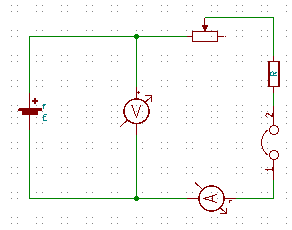
This experiment includes the above mentioned circuitry. Once the basic setup is completed using; Dry cell 10K variable resistor 1K resistor Switch/Jumper Connect the CH1 pin and GND pin of PSLab across the dry cell and CH2 pin and GND across the Ammeter instead of the Ammeter. Once the pin connection is complete, plug the PSLab device to the computer and using the desktop application voltmeter, measure the voltage from CH1 and current from voltage value read from CH2 and the known resistance value of R. Record these data against step changes in the resistance of the variable resistor starting from a high value to a low value. Once there are sufficient data as much as 10 data set, using a graph paper draw the relation between current and voltage measured according to the equation given below. E = V + Ir V = -rI + E This will produce a graph with a constant negative gradient. Gradient of the graph will produce the internal resistance of the dry cell. I-V graphs for a semiconductor This experiment will require; Diode 100 Ohms resistor Conduct the experiment as follows once the circuit is set up. Increase the voltage provided by the PV1 pin of the PSLab by 100 mV per step and measure the voltage across diode using CH3 pin of PSLab device. Using that voltage and the supply voltage, calculate the current flowing through the resistor. Note down the readings as voltage to current pairs and plot them on a graph paper. The graph will produce the following results which is identical to common IV characteristics of a semiconductor. Start A at zero and increase by 0.1V steps while measuring voltage and current across diode. (Image from Wikipedia) Apart from this conventional experiment, PSLab provides an inbuilt experiment students and teachers can use. In the Electronics Experiments section, Diode IV characteristics experiment is configured in such a way that this experiment can be conducted very easily. The circuit configuration is the same and R value should be 1K. Once the step size is set to an appropriate resolution, START button will begin the experiment and provide with the final graph. Transfer characteristics of a transistor Set up the…

Continue ReadingHigh School Physics Practicals using PSLab Device