Creating step designs from KiCAD for PSLab

PSLab hardware device is developed using KiCAD. It is an open source PCB designing tool which we can use for free and it has almost all the features needed to build a professional PCB. But it lacks one thing. It cannot generate and export 3D models. In fact there is a 3D viewer in KiCAD but there is no way to export it. When manufacturing PSLab devices, it was required by the manufacturers so that they can have a clear understanding how the components are placed. This step is necessary for them to design the production line.

Before we get started, there are few prerequisites to help us get this done. They are as follows;

  1. FreeCAD: Open source 3D modeling software
  2. KiCAD step up tools: External library to import KiCAD PCB layouts to FreeCAD

You may need to follow installation instructions to install FreeCAD from the link given. Once we are all set, extract the KiCAD Stepup tools. There we can find a set of python libraries and some bash scripts. We can either use the scripts or type commands ourselves. I found scripts having some issues configuring paths.

To fire up FreeCAD with KiCAD stepup tools enabled, type the following command on your console;

$ freecad kicad-StepUp-tools.FCMacro
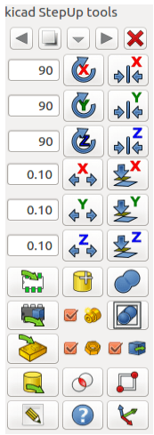
Make sure the console is pointing to the directory where the FCMacro file is located. This will open up FreeCAD and if you opened it already and saw the opening screen of FreeCAD, you’d notice a whole new toolbar is added.

Here you can see many tools related to import and export step files and 3D models from outside libraries and folders. Each tool is specific;

  • Load-kicad-footprint:

This tool is useful to generate a step file for an individual PCB component, say a resistor into a step file.

  • Export-to-kicad:

There are instances where when we design a custom foot print, and KiCAD doesn’t have the 3D model. In such a case we can export such a model to KiCAD

  • Load-kicad:

This is the tool we are using to export PSLab PCB board to step format. Before we move on to this tool there is one last configuration we have to do. FreeCAD doesn’t know where we have put KiCAD 3D models. This library simply transforms the available 3D models in KiCAD into step files and build the final output combining all of them together as in the featured image of this blog post. To setup the 3D model path, in KiCAD, there is a path configuration option. Copy the path under “KISYS3DMOD”.
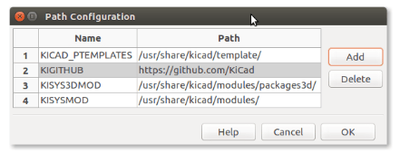
Figure 2: Path Configuration dialog box in KiCAD

And paste it into the ini file named “ksu-config.ini” which you can find in home folder.

Figure 3: Place to add 3D model path in ksu-config.ini file

Once that is done, click on the Load-KiCAD tool icon and browse to the repository where the PSLab hardware files are located at. Open the board file and FreeCAD will generate part by part and finally output the complete design. Now we can export the design in plenty of formats such as steps, stl another similar file format and many more.

Reference:

  1. https://www.freecadweb.org/wiki/Download
  2. http://kicad-pcb.org/external-tools/stepup/
Continue ReadingCreating step designs from KiCAD for PSLab

Creating Logos for PSLab with KiCAD

We can make plenty of PCB designs using KiCAD, a powerful open source CAD tool. What makes them unique is customized logos and brand names. KiCAD offers us a feature to add logos in any of the silk screens; bottom or top. Rather than just a textual logos, a graphical logo makes the design look more unique just like the PSLab v5 revision.

The process is not a tedious task. We can simply start by getting the logo we want to add in the PCB silk screen. Just to make it more clear, silk screen is a paint made on top of the circuit board with all the markings and labels with a special ink. It will be either white or black according to user preference. As the first step, open the logo image file with inkscape.

We need to pre-process the image before we move onto KiCAD development space. The silk screen will have a black and white image as the input. It will convert all the black parts to invisible and white parts visible in the silk screen color. In that sense we have to color transform any logo into following format to get the desired output.

Once the logo image is ready, open KiCAD and from it’s toolbar;

Click and open “Bitmap2Component” icon which is similar to a “simple a”. This will open a window where you can import the logo image in png format.

In this figure, image height and width is massive. It is always a good practice to have a large image and then scale it down to prevent any detail losses. If the image is too big, from the “Resolution” section, try increasing the DPI value and observe the dimensions are shrinking. You can have a ruler and measure the actual size of the image you want and then adjust the DPI values to get the desired dimensions. In my case I had to use 2500×3000 DPI to get an image of 20mmx7mm,

The next step is to export the logo file. Click on the “Export” button and select the location to your custom component library and save the file in “kicad_mod” format.

Now open up “Pcbnew” layout where the PCB design is. From the toolbar to your right, click on the “Add footprint” icon.

A dialog box will pop up to select the component. Click on the button “Select by Browser” to get a more interactive selection menu or you can simply type the name if you remember it correctly.

From the component browser, browse to the library where you saved the kicad_mod file and import it to the layout. The final result will look like this. If the dimensions are not what you wanted, simply follow the previous steps again to increase the DPI values to get the correct dimensions. By pressing “f” you can flip the silk screen side, bottom or top to place the logo where ever you want.

Reference:

KiCAD Documentation: http://kicad-pcb.org/help/documentation/

Continue ReadingCreating Logos for PSLab with KiCAD

Circuit Protection Measurements in PSLab Hardware

Pocket Science Lab by FOSSASIA is a versatile analytical tool which can be used by a variety of user. They span from school kids to professional engineers who need a measurement device to ease up their task. In electronics and electrical fields, circuits do get damaged a lot. There is no perfect method to keep the circuit damage proof but the only thing we can do it minimize the damaging causes as much as possible. PSLab is no exception.

Since PSLab has an audience involving school children, it is quite possible for a short circuit to happen in devices while using. A short circuit is simply a non-resistive path between a supply pin and a ground connection. When a short circuit happens, there is a huge amount of electrons flowing through a small path which will eventually melts if there is no safety mechanism to stop the rapid electron flow.

PSLab contains a plenty of sensitive integrated circuits to support its wide variety of features. They will easily burn if a short happens and the user will have to dispose the device as it will no longer be functional. That is the case if there is no safety feature embedded in the printed circuit board to fight against damages of that nature. We have included a special type of fuses to overcome damages occur due to short circuits.

A fuse is a passive component which allows the flow of current up to a threshold value. When the current increases, the fuse blows and the flow is disrupted. A normal fuse will require replacement. But in PSLab, we have included a special type of fuse known as a polyfuse. This type of fuse does not require replacement. In the following figure it is shown as “F1”

Figure 1: Position of fuse in PSLab V4 PCB

The speciality about poly fuses is that they will recover its current carrying capabilities once the short circuit is open. The auxiliary name “Resettable Fuse” will make sense as it will reset to its original state once the circuit is safe.

The working principle behind a polyfuse mainly depends on its resistance. When the current flow through a polyfuse is at the rated values, it will have a minimum resistance between the input and output terminals.

Figure 2: A poly fuse

As the current flow increases, the particles inside the fuse will start moving fast. The slow motion of these particles are the ones keeping a smooth current flow across the fuse. When the particles are moving rapidly, it will oppose the current flow through them.

Imagine a situation where a short circuit happens. There will be sudden rapid flow of electrons. These electrons will collide with the particles inside polyfuse which were at a calm and steady motion. Now their motion is disturbed and the movements will be random and fast. This will cause the fuse to heat up to a high temperature. As the graph in figure 3 illustrates, it’s resistance highly increases with the temperature.

Figure 3: Temperature vs Current graph of a poly fuse

The rapid electron flow will have no opening to go as the fuse path is now heavily resistive. When the current flow is stopped, PSLab will turn off. All these things happen so quickly that the short circuit would not damage any internal components anymore. Once the user sees that the PSLab is off and he solves the cause for the short circuit, the fuse will cool down which results in a lesser resistance. Now the current flow will come back to normal making the PSLab device working again.

Reference:

Polyfuse – Mouser: https://www.mouser.com/datasheet/2/240/Littelfuse_PTC_LoRho_Datasheet.pdf-365270.pdf

Continue ReadingCircuit Protection Measurements in PSLab Hardware

How to get a cost effective PCB for Production

Designing a PCB for a DIY project involves in making up the schematics which then turned into a PCB layout. Components used in these PCBs will be mostly “Through Hole” which are commonly available in the market. Once the PCB is printed in either screen printing techniques or using photo resistive dry films, making alterations to the component mounting pads and connections will be somewhat possible.

When dealing with a professional PCB design, there are many properties we need to consider. DIY PCBs will simply be single sided in most cases. A professional printed circuit board will most likely to have more than one layer. The PCB for PSLab device has 4 layers. Adding more layers to a PCB design makes it easier to draw connections. But on the other hand, the cost will increase exponentially. The designer must try to optimize the design to have less layers as much as possible. The following table shows the estimated cost for printing for 10 PSLab devices if the device had that many layers.

One Layer Two Layers Four Layers Six Layers
$4.90 $4.90 $49.90 $305.92

Once the layer levels increase from 2, the other layers will be inner layers. The effective area of inner layers will be reduced if the designer adds more through hole components or vias which connects a connection from a one layer with a connection with another layer. The components used will then be limited to surface mount components.

Surface Mount components (SMD) are expensive compared to their Through Hole (TH) counterpart. But the smaller size of SMD makes it easier to place many components in a smaller area than to Through Hole components. Soldering and assembling Through Hole components can be done manually using hand soldering techniques. SMD components need special tools and soldering equipments to assemble and solder them. Much more precision is required when SMD components are soldered. Hence automated assembly is used in industry where robot arms are used to place components and reflow soldering techniques to solder the SMD components. This emphasizes that the number of SMD components used in the PCB will increase the assembly cost as well as the component cost but it will greatly reduce the size of the PCB.

SMD components comes in different packages. Passive components such as resistors, capacitors will come in 0.25 mm upto 7.4mm dimensions. PSLab device uses 0805/2012 sized package which is easier to find in the market and big enough to pick and assemble by hand. The packaging refers to its dimensions. 0805 reads as 0.08 inches long and 0.05 inches wide.

Finding the components in the market is the next challenging task. We can easily purchase components from an online store but the price will be pretty high. If the design can spare some space, it will be wise to have alternative pads for a Through Hole component for the SMD component as Through Hole components can be found much easier than SMD components in a local store.

The following image is taken from Sparkfun which illustrates different common IC packages. Selecting the correct footprint for the SMD IC and vise versa is very important. It is a good practice to check the stores for the availability and prices for the components before finalizing the PCB design with footprints and sending it to printing. We may find some ICs are not available for immediate purchase as the stocks ran out but a different package of the same IC is available. Then the designer can alter the foot print to the packaging and use the more common packaging type in the design.

Considering all the factors above, a cost effective PCB can be designed and manufactured once the design is optimized to have the minimum number of layers with components with the minimum cost for both assembly and components.

Resources:

Continue ReadingHow to get a cost effective PCB for Production

Creating Bill of Materials for PSLab using KiCAD

PSLab device consists of a hundreds of electronic components. Resistors, diodes, transistors, integrated circuits are to name a few. These components are of two types; Through hole and surface mounted.

Surface mount components (SMD) are smaller in size. Due to this reason, it is hard to hand solder these components onto a printed circuit board. We use wave soldering or reflow soldering to connect them with a circuit.

Through Hole components (TH) are fairly larger than their SMD counter part. They are made bigger to make it easy for hand soldering. These components can also be soldered using wave soldering.

Once a PCB has completed its design, the next step is to manufacture it with the help of a PCB manufacturer. They will require the circuit design in “gerber” format along with its Bill of Materials (BoM) for assembly. The common requirement of BoM is the file in a csv format. Some manufacturers will require the file in xml format. There are many plugins available in KiCAD which does the job.

KiCAD when first installed, doesn’t come configured with a BoM generation tool. But there are many scripts developed with python available online free of charge. KiBoM is one of the famous plugins available for the task.

Go to “Eeschema” editor in KiCAD where the schematic is present and then click on the “BoM” icon in the menu bar. This will open a dialog box to select which plugin to use to generate the bill of materials.

Initially there won’t be any plugins available in the “Plugins” section. As we are adding plugins to it, they will be listed down so that we can select which plugin we need. To add a plugin, click on the “Add Plugin” button to open the dialog box to browse to the specific plugin we have already downloaded. There are a set of available plugins in the KiCAD installation directory.

The path is most probably will be (unless you have made any changes to the installation);

usr/lib/kicad/plugins

Once a plugin is selected, click on “Generate” button to generate the bom file. “Plugin Info” will display where the file was made and it’s name.

Make sure we have made the BoM file compatible to the file required by the manufacturer. That is; removed all the extra content and added necessary details such as manufacturer’s part numbers and references replacing the auto generated part numbers.

Resources:

Continue ReadingCreating Bill of Materials for PSLab using KiCAD