Building PSLab Android app with Fdroid

Fdroid is a place for open source enthusiasts and developers to host their Free and Open Source Software (FOSS) for free and get more people onboard into their community. Hosting an app in Fdroid is not a fairly easy process just like hosting one in Google Play. We need to perform a set of build checks prior to making a merge request (which is similar to pull request in GitHub) in the fdroid-data GitLab repository. PSLab Android app by FOSSASIA has undergone through all these checks and tests and now ready to be published.

Setting up the fdroid-server and fdroid-data repositories is one thing. Building our app using the tools provided by fdroid is another thing. It will involve quite a few steps to get started. Fdroid requires all the apps need to be built using:

$ fdroid build -v -l org.fossasia.pslab


This will output a set of logs which tell us what went wrong in the builds. The usual one in a first time app is obviously the build is not taking place at all. The reason is our metadata file needs to be changed to initiate a build.

Build:<versioncode>,<versionname>
    commit=<commit which has the build mentioned in versioncode>
    subdir=app
    gradle=yes


When a metadata file is initially created, this build is disabled by default and commit is set to “?”. We need to fill in those blanks. Once completed, it will look like the snippet above. There can be many blocks of “Build” can be added to the end of metadata file as we are advancing and upgrading through the app. As an example, the latest PSLab Android app has the following metadata “Build” block:

Build:1.1.5,7
    commit=0a50834ccf9264615d275a26feaf555db42eb4eb
    subdir=app
    gradle=yes


In case of an update, add another “Build” block and mention the version you want to appear on the Fdroid repository as follows:

Auto Update Mode:Version v%v
Update Check Mode:Tags
Current Version:1.1.5
Current Version Code:7


Once it is all filled, run the build command once again. If you have properly set the environment in your local PC, build will end successfully assuming there were no Java or any other language syntax errors.

It is worth to mention few other facts which are common to Android software projects. Usually the source code is packed in a folder named “app” inside the repository and this is the common scenario if Android Studio builds up the project from scratch. If this “app” folder is one level below the root, that is “android/app”, the build instructions shown above will throw an error as it cannot find the project files.

The reason behind this is we have mentioned “subdir=app” in the metadata file. Change this to “subdir=android/app” and run the build again. The idea is to direct the build to find where the project files are.

Apart from that, the commit can be represented by a tag instead of a long commit hash. As an example, if we had merge commits in PSLab labeled as “v.<versioncode>”, we can simply use “commit=v.1.1.5” instead of the hash code. It is just a matter of readability.

Happy Coding!

Reference:

  1. Metadata : https://f-droid.org/docs/Build_Metadata_Reference/#Build
  2. PSLab Android app Fdroid : https://gitlab.com/fdroid/fdroiddata/merge_requests/3271/diffs
Continue ReadingBuilding PSLab Android app with Fdroid

Creating Device Screen to show connection status of PSLab Device

For using the PSLab Device the user needs to connect the PSLab device to an Android Phone having a PSLab android app. So there should be a screen that should be able to show the proper status of the PSLab device connection to the android app dynamically and it should also contain instructions on “How to connect the device to the app”.

So, in this blog we will create a device screen which shows the proper status of the connection of the PSLab device with the phone.

First step will be designing the layout for the device screen, for this we will create a fragment named HomeFragment and for its layout we will make use of the Relative Layout as view group and then create a Linearlayout inside it and position it at the center so that it always appears at the center in different screen sizes.

Then inside the LinearLayout, we will create(as shown in respective order) :

  1. ImageView and TextView for showing the status of device connection.
  2. Linear Layout with multiple TextView showing instructions on “How to connect the device to the screen”.
  3. A TextView that will direct the user to a webview showing PSLab website.

After creating all the above views we have created the layout will look like this: –

Now for showing the PSLab connection status dynamically, we have to implement following logic:

  1. When the device is connected it should show the connected icon and text and hide the instructions.
  2. When the device is disconnected it should show the disconnected icon and text and also the instructions.

For this, we will create a method inside the HomeFragment Java file which make use of Arguments deviceConnected and deviceFound to store device connected status.

public static HomeFragment newInstance(boolean deviceConnected, boolean deviceFound) {
HomeFragment homeFragment = new HomeFragment();
homeFragment.deviceConnected = deviceConnected;
homeFragment.deviceFound = deviceFound;
return homeFragment;
}

When both arguments are true we will show the connected text and icon and hide the instructions.

And when both arguments are false we will show the disconnected text and icon and display the instructions.

if (deviceFound && deviceConnected) {
   tvConnectMsg.setVisibility(View.GONE);
   tvVersion.setText(scienceLab.getVersion());
   tvVersion.setVisibility(View.VISIBLE);
   imgViewDeviceStatus.setImageResource(R.drawable.icons8_usb_connected_100);
   tvDeviceStatus.setText(getString(R.string.device_connected_successfully));
} else {
 imgViewDeviceStatus.setImageResource(R.drawable.icons_usb_disconnected_100);
 tvDeviceStatus.setText(getString(R.string.device_not_found));
}

How do we know that the device is connected?

For this, we have to handle the USB Attach event [1] that is whenever the USB is connected the Android will give a broadcast of USB connected and on receiving that broadcast in the app we will replace the HomeFragment giving setting both arguments to true. 

We will create a Broadcast Receiver[2] in the main activity which executes it’s onReceive() method on receiving USB attach event.

private final BroadcastReceiver mUsbReceiver = new BroadcastReceiver() {
   public void onReceive(Context context, Intent intent) {
     String action = intent.getAction();
     if (UsbManager.ACTION_USB_DEVICE_ATTACHED.equals(action)) {
       UsbDevice device =  intent.getParcelableExtra(UsbManager.EXTRA_DEVICE);
       if(device!=null){                                                  
         getSupportFragmentManager().beginTransaction().replace(R.id.frame,                                            
           HomeFragment.newInstance(true, true)).commitAllowingStateLoss();
         }           
      }
   }
};

Here In the OnReceive Method, we will replace our device screen fragment by passing parameters deviceConnected = true and deviceFound = true to HomeFragment newInstance() method.

Every time we create a Receiver we have to bind corresponding intent filters with broadcast receivers when the application is created.

IntentFilter filter = new IntentFilter(UsbManager.ACTION_USB_DEVICE_ATTACHED);
registerReceiver(mUsbReceiver, filter);

Similarly, we also have to handle the USB Detach event [2], here we will create a Broadcast Receiver[2] which executes in onReceive() method whenever the device is detached and here inside onReceive() method we will replace our device screen by passing parameters deviceConnected = false and deviceFound = false to newInstance() method in HomeFragment.

private final BroadcastReceiver mUsbReceiver = new BroadcastReceiver() {
   public void onReceive(Context context, Intent intent) {
     String action = intent.getAction();
     if (UsbManager.ACTION_USB_DEVICE_DETACHED.equals(action)) {                                           
getSupportFragmentManager().beginTransaction().replace(R.id.frame,                                            
           HomeFragment.newInstance(false, false)).commitAllowingStateLoss();
         }           
      }
   }
};

Thus, as shown in fig. 2 we have shown the PSLab device connection status dynamically on the screen by handling the USB attach/detach events.

Figure 2 shows the UI of ‘Device Screen’ for the two possible status: ‘not connected’ and ‘connected’

Resources

  1. Codepool Blog – “How to monitor USB events on Android?” by Xiao Ling
  2. Vogella article “What is Broadcast Receiver and how to insert it your app?”
Continue ReadingCreating Device Screen to show connection status of PSLab Device

Publish an Open Source app on Fdroid

Fdroid is a famous software repository hosted with numerous free and open source Android apps. They have a main repository where they allow developers hosting free and ad free software after a thorough check up on the app. This blog will tell you how to get your project hosted in their repository using steps I followed to publish the PSLab Android app.

Before you get started, make sure you have the consent from your developer community to publish their app on Fdroid. Fdroid requires your app to use all kind of open resources to implement features. If there is any closed source libraries in your app and you still want to publish it on Fdroid, you may have to reimplement that feature by any other mean without using closed source resources. They will also not allow to have Google’s proprietary “play-services” in your app along with proprietary ad services. You can find the complete inclusion policy document from their official page.

When your app is fully ready, you can get started with the inclusion procedure. Unlike how we are publishing apps on Google Play, publishing an app on Fdroid is as simple as sending a pull request to their main repository. That’s exactly what we have to do. In simple terms all we have to do is:

  1. Fork the Fdroid main data repository
  2. Make changes to their files to include our app
  3. Do a pull request

First of all you need a GitLab account as the Fdroid repository is hosted in GitLab. Once you are ready with a GitLab account, fork and clone the f-droid-data repository. The next step is to install the fdroid-server. This can be simply done using apt:

$ sudo apt install fdroidserver

Once that is done, go into the directory where you cloned the repository and run the following command to read current meta data where it saves all the information related to existing apps on Fdroid;

$ fdroid readmeta

This will list out various details about the current meta files. Next step is to add our app details into this meta file. This can be done easily using following command or you can manually create folders and files. But the following is safer;

$ fdroid import --url https://github.com/fossasia/pslab-android --subdir app

Replace the link to repository from the –url tag in the above command. For instance the following will be the link for fossasia-phimpme android;

$ fdroid import --url https://github.com/fossasia/phimpme-android --subdir app

This will create a file named as “org.fossasia.pslab” in the metadata directory. Open up this text file and we have to fill in our details.

  1. Categories
  2. License
  3. Web Site
  4. Summary
  5. Description

Description needs to be terminated with a newline and a dot to avoid build failures.

Once the file is filled up, run the following command to make sure that the metadata file is complete.

$ fdroid readmeta

Then run the following command to clean up the file

$ fdroid rewritemeta org.fossasia.pslab

We can automatically add version details using the following command:

$ fdroid checkupdates org.fossasia.pslab

Now run the lint test to see if the app is building correctly.

$ fdroid lint org.fossasia.pslab

If there are any errors thrown, fix them to get to the next step where we actually build the app:

$ fdroid build -v -l org.fossasia.pslab

Now you are ready to make the pull request which will then get reviewed by developers in Fdroid community to get it merged into their main branch. Make a commit and then push to your fork. From there it is pretty straightforward to make a pull request to the main repository. Once that is done, they will test the app for any insecurities. If all of them are passed, the app will be available in Fdroid!

Reference:

  1. Quick Start: https://gitlab.com/fdroid/fdroiddata/blob/master/README.md#quickstart
  2. Making merge requests: https://gitlab.com/fdroid/fdroiddata/blob/master/CONTRIBUTING.md#merge-requests
Continue ReadingPublish an Open Source app on Fdroid

Creating Logos for PSLab with KiCAD

We can make plenty of PCB designs using KiCAD, a powerful open source CAD tool. What makes them unique is customized logos and brand names. KiCAD offers us a feature to add logos in any of the silk screens; bottom or top. Rather than just a textual logos, a graphical logo makes the design look more unique just like the PSLab v5 revision.

The process is not a tedious task. We can simply start by getting the logo we want to add in the PCB silk screen. Just to make it more clear, silk screen is a paint made on top of the circuit board with all the markings and labels with a special ink. It will be either white or black according to user preference. As the first step, open the logo image file with inkscape.

We need to pre-process the image before we move onto KiCAD development space. The silk screen will have a black and white image as the input. It will convert all the black parts to invisible and white parts visible in the silk screen color. In that sense we have to color transform any logo into following format to get the desired output.

Once the logo image is ready, open KiCAD and from it’s toolbar;

Click and open “Bitmap2Component” icon which is similar to a “simple a”. This will open a window where you can import the logo image in png format.

In this figure, image height and width is massive. It is always a good practice to have a large image and then scale it down to prevent any detail losses. If the image is too big, from the “Resolution” section, try increasing the DPI value and observe the dimensions are shrinking. You can have a ruler and measure the actual size of the image you want and then adjust the DPI values to get the desired dimensions. In my case I had to use 2500×3000 DPI to get an image of 20mmx7mm,

The next step is to export the logo file. Click on the “Export” button and select the location to your custom component library and save the file in “kicad_mod” format.

Now open up “Pcbnew” layout where the PCB design is. From the toolbar to your right, click on the “Add footprint” icon.

A dialog box will pop up to select the component. Click on the button “Select by Browser” to get a more interactive selection menu or you can simply type the name if you remember it correctly.

From the component browser, browse to the library where you saved the kicad_mod file and import it to the layout. The final result will look like this. If the dimensions are not what you wanted, simply follow the previous steps again to increase the DPI values to get the correct dimensions. By pressing “f” you can flip the silk screen side, bottom or top to place the logo where ever you want.

Reference:

KiCAD Documentation: http://kicad-pcb.org/help/documentation/

Continue ReadingCreating Logos for PSLab with KiCAD

Circuit Protection Measurements in PSLab Hardware

Pocket Science Lab by FOSSASIA is a versatile analytical tool which can be used by a variety of user. They span from school kids to professional engineers who need a measurement device to ease up their task. In electronics and electrical fields, circuits do get damaged a lot. There is no perfect method to keep the circuit damage proof but the only thing we can do it minimize the damaging causes as much as possible. PSLab is no exception.

Since PSLab has an audience involving school children, it is quite possible for a short circuit to happen in devices while using. A short circuit is simply a non-resistive path between a supply pin and a ground connection. When a short circuit happens, there is a huge amount of electrons flowing through a small path which will eventually melts if there is no safety mechanism to stop the rapid electron flow.

PSLab contains a plenty of sensitive integrated circuits to support its wide variety of features. They will easily burn if a short happens and the user will have to dispose the device as it will no longer be functional. That is the case if there is no safety feature embedded in the printed circuit board to fight against damages of that nature. We have included a special type of fuses to overcome damages occur due to short circuits.

A fuse is a passive component which allows the flow of current up to a threshold value. When the current increases, the fuse blows and the flow is disrupted. A normal fuse will require replacement. But in PSLab, we have included a special type of fuse known as a polyfuse. This type of fuse does not require replacement. In the following figure it is shown as “F1”

Figure 1: Position of fuse in PSLab V4 PCB

The speciality about poly fuses is that they will recover its current carrying capabilities once the short circuit is open. The auxiliary name “Resettable Fuse” will make sense as it will reset to its original state once the circuit is safe.

The working principle behind a polyfuse mainly depends on its resistance. When the current flow through a polyfuse is at the rated values, it will have a minimum resistance between the input and output terminals.

Figure 2: A poly fuse

As the current flow increases, the particles inside the fuse will start moving fast. The slow motion of these particles are the ones keeping a smooth current flow across the fuse. When the particles are moving rapidly, it will oppose the current flow through them.

Imagine a situation where a short circuit happens. There will be sudden rapid flow of electrons. These electrons will collide with the particles inside polyfuse which were at a calm and steady motion. Now their motion is disturbed and the movements will be random and fast. This will cause the fuse to heat up to a high temperature. As the graph in figure 3 illustrates, it’s resistance highly increases with the temperature.

Figure 3: Temperature vs Current graph of a poly fuse

The rapid electron flow will have no opening to go as the fuse path is now heavily resistive. When the current flow is stopped, PSLab will turn off. All these things happen so quickly that the short circuit would not damage any internal components anymore. Once the user sees that the PSLab is off and he solves the cause for the short circuit, the fuse will cool down which results in a lesser resistance. Now the current flow will come back to normal making the PSLab device working again.

Reference:

Polyfuse – Mouser: https://www.mouser.com/datasheet/2/240/Littelfuse_PTC_LoRho_Datasheet.pdf-365270.pdf

Continue ReadingCircuit Protection Measurements in PSLab Hardware

Implementing Clickable Images

PSLab Android application is a feature rich compact app to user interface the PSLab hardware device. Similarly the PSLab device itself is a compact device with a plenty of features to replace almost all the analytical instruments in a school science lab. When a first time user takes the device and connect it with the Android app, there are so many pins labeled with abbreviations. This creates lots of complications unless the user checks the pinout diagram separately.

As a workaround a UI is proposed to integrate a layout containing the PSLab PCB image where user can click on each pin to get a dialog box explaining him what that specific pin is and what it does. This implementation can be done it two ways;

  • Using an Image map
  • Using (x,y) coordinates

The first implementation is more practical and can be applied with any device with any dimension. The latter requires some transformation to capture the correct position when user has clicked on a pin. So the first method will be implemented.

The idea behind using an image map is to have two images with exact dimensions on top of each other. The topmost image will be the color map which we create ourselves using unique colors at unique heat points. This image will have the visibility setting invisible as the main idea is to let the  user see a meaningful image and capture the positions using a secondary in the back end.

To make things much clear, let’s have a look at a color map image I am suggesting here for a general case.

If we overlap the color map with the PSLab layout, we will be able to detect where user has clicked using Android onTouchEvent.

@Override
public boolean onTouchEvent(MotionEvent ev) {
   final int action = ev.getAction();
   final int evX = (int) ev.getX();
   final int evY = (int) ev.getY();
   switch (action) {
       case MotionEvent.ACTION_UP :
         int touchColor = getHotspotColor (R.id.backgroundMap, evX, evY);
         /* Display the relevant pin description dialog box here */
         break;
   }
   return true;
}

 
Color of the clicked position can be captured using the following code;

public int getHotspotColor (int hotspotId, int x, int y) {
   ImageView img = (ImageView) findViewById (hotspotId);
   img.setDrawingCacheEnabled(true);
   Bitmap hotspots = Bitmap.createBitmap(img.getDrawingCache());
   img.setDrawingCacheEnabled(false);
   return hotspots.getPixel(x, y);
}

 
If we go into details, from the onTouchEvent we capture the (x,y) coordinates related to user click. Then this location is looked up for a unique color by creating a temporary bitmap and then getting the pixel value at the captured coordinate.

There is an error in this method as the height parameter always have an offset. This offset is introduced by the status bar and the action bar of the application. If we use this method directly, there will be an exception thrown out saying image height is less than the height defined by y.

Solving this issue involves calculating status bar and actionbar heights separately and then subtract them from the y coordinate.

Actionbar and status bar heights can be calculated as follows;

Rect rectangle = new Rect();
Window window = getWindow();
window.getDecorView().getWindowVisibleDisplayFrame(rectangle);
int statusBarHeight = rectangle.top;
int contentViewTop = window.findViewById(Window.ID_ANDROID_CONTENT).getTop();
int titleBarHeight= contentViewTop - statusBarHeight;

 
Using them, we can modify the captured coordinates as follows;

int touchColor = getHotspotColor (R.id.imageArea, evX, evY - statusBarHeight);

 
This way the exception is handled by adjusting the cursor position. Once this is done, it is all about displaying the correct pin description dialog box.

Reference:

Calculate status bar height: https://stackoverflow.com/questions/3407256/height-of-status-bar-in-android

Continue ReadingImplementing Clickable Images

Making Shapes with PSLab Oscilloscope

Looking back to history, the first ever video game was ‘Pong’ which was played on an analog oscilloscope with a very small screen. Oscilloscopes are not made to play video games, but by just tinkering around its basic functionality which is display waveforms, we can do plenty of cool things. PSLab device also has an oscilloscope; in fact it’s a four channel oscilloscope.

This blog post will show you how the oscilloscope in PSLab is not just a cheap oscilloscope but it has lots of functionalities an industry grade oscilloscope has (except for the bandwidth limitation to a maximum of 2 MHz)

To produce shapes like above figures, we are using another instrument available in PSLab. That is ‘Waveform Generator’. PSLab Waveform Generator can generate three different waveforms namely Sine waves, Triangular waves and Square waves ranging from 5 Hz to 5 kHz.

To get started, first connect two jumper wires between SI1-CH1 and SI2-CH2 pins. We needn’t worry about ground pins as they are already internally connected. Now it’s time to open up the PSLab oscilloscope. Here we are going to utilize two channels for this activity and they will be CH1 and CH2. Check the tick boxes in front of ‘Chan 1’ and ‘Chan 2’ and set ‘Range’ to “+/-4V” to have the maximum visibility filling the whole screen with the waveform.

The shapes are drawn using a special mode called ‘X-Y Mode’ in PSLab oscilloscope. In this mode, two channels will be plotted against their amplitudes at every point in time.

As it is already mentioned that PSLab can generate many waveform types and also they can have different phase angles relative to each other. They can have different independent frequencies. With all these combinations, we can tweak the settings in Waveform Generator to produce different cool shapes in PSLab oscilloscope.

These shapes can vary from basic geometric shapes such as circle, square, rectangle to complicated shapes such as rhombus, ellipse and polynomial curves.

Circle

A circular shape can be made by generating two sine waves having the same frequency but with a phase difference of 90 degrees or 270 degrees between the two wave forms.


Square

Square shape can be made by generating two triangular waveforms again having the same frequency but with a phase difference of either 90 degrees or 270 degrees between the two.


Rectangle

Similar to creating a Square, by having the same frequency for both triangular waveforms but a different phase angle greater than or less than 90 degree will do the trick.


Rhombus

Keeping the waveform settings same for the rectangle, by changing the amplitude of the SI1 waveform using the knob we can generate a rhombic shape on the XY graph plot.


Ellipse

Generating ellipse is also similar to creating a rhombus. But here we are using sine waves instead of triangular waves. By changing the amplitude of SI1 using the knob we can change the curvature.


Helix

Helix or spiral shape can be generated using two sine waves having same phase but two different frequencies. Frequencies better be integer multiples of the smaller frequency to  have a steady shape.


Parabola

Parabolic shapes can be generated by mixing up triangular waves with sine waves with different phase angles.


More random shapes


References:

https://www.aps.org/publications/apsnews/200810/physicshistory.cfm

Continue ReadingMaking Shapes with PSLab Oscilloscope

How to get a cost effective PCB for Production

Designing a PCB for a DIY project involves in making up the schematics which then turned into a PCB layout. Components used in these PCBs will be mostly “Through Hole” which are commonly available in the market. Once the PCB is printed in either screen printing techniques or using photo resistive dry films, making alterations to the component mounting pads and connections will be somewhat possible.

When dealing with a professional PCB design, there are many properties we need to consider. DIY PCBs will simply be single sided in most cases. A professional printed circuit board will most likely to have more than one layer. The PCB for PSLab device has 4 layers. Adding more layers to a PCB design makes it easier to draw connections. But on the other hand, the cost will increase exponentially. The designer must try to optimize the design to have less layers as much as possible. The following table shows the estimated cost for printing for 10 PSLab devices if the device had that many layers.

One Layer Two Layers Four Layers Six Layers
$4.90 $4.90 $49.90 $305.92

Once the layer levels increase from 2, the other layers will be inner layers. The effective area of inner layers will be reduced if the designer adds more through hole components or vias which connects a connection from a one layer with a connection with another layer. The components used will then be limited to surface mount components.

Surface Mount components (SMD) are expensive compared to their Through Hole (TH) counterpart. But the smaller size of SMD makes it easier to place many components in a smaller area than to Through Hole components. Soldering and assembling Through Hole components can be done manually using hand soldering techniques. SMD components need special tools and soldering equipments to assemble and solder them. Much more precision is required when SMD components are soldered. Hence automated assembly is used in industry where robot arms are used to place components and reflow soldering techniques to solder the SMD components. This emphasizes that the number of SMD components used in the PCB will increase the assembly cost as well as the component cost but it will greatly reduce the size of the PCB.

SMD components comes in different packages. Passive components such as resistors, capacitors will come in 0.25 mm upto 7.4mm dimensions. PSLab device uses 0805/2012 sized package which is easier to find in the market and big enough to pick and assemble by hand. The packaging refers to its dimensions. 0805 reads as 0.08 inches long and 0.05 inches wide.

Finding the components in the market is the next challenging task. We can easily purchase components from an online store but the price will be pretty high. If the design can spare some space, it will be wise to have alternative pads for a Through Hole component for the SMD component as Through Hole components can be found much easier than SMD components in a local store.

The following image is taken from Sparkfun which illustrates different common IC packages. Selecting the correct footprint for the SMD IC and vise versa is very important. It is a good practice to check the stores for the availability and prices for the components before finalizing the PCB design with footprints and sending it to printing. We may find some ICs are not available for immediate purchase as the stocks ran out but a different package of the same IC is available. Then the designer can alter the foot print to the packaging and use the more common packaging type in the design.

Considering all the factors above, a cost effective PCB can be designed and manufactured once the design is optimized to have the minimum number of layers with components with the minimum cost for both assembly and components.

Resources:

Continue ReadingHow to get a cost effective PCB for Production

Creating Bill of Materials for PSLab using KiCAD

PSLab device consists of a hundreds of electronic components. Resistors, diodes, transistors, integrated circuits are to name a few. These components are of two types; Through hole and surface mounted.

Surface mount components (SMD) are smaller in size. Due to this reason, it is hard to hand solder these components onto a printed circuit board. We use wave soldering or reflow soldering to connect them with a circuit.

Through Hole components (TH) are fairly larger than their SMD counter part. They are made bigger to make it easy for hand soldering. These components can also be soldered using wave soldering.

Once a PCB has completed its design, the next step is to manufacture it with the help of a PCB manufacturer. They will require the circuit design in “gerber” format along with its Bill of Materials (BoM) for assembly. The common requirement of BoM is the file in a csv format. Some manufacturers will require the file in xml format. There are many plugins available in KiCAD which does the job.

KiCAD when first installed, doesn’t come configured with a BoM generation tool. But there are many scripts developed with python available online free of charge. KiBoM is one of the famous plugins available for the task.

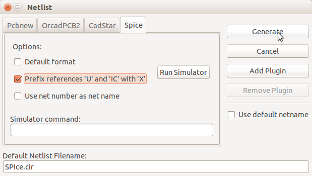
Go to “Eeschema” editor in KiCAD where the schematic is present and then click on the “BoM” icon in the menu bar. This will open a dialog box to select which plugin to use to generate the bill of materials.

Initially there won’t be any plugins available in the “Plugins” section. As we are adding plugins to it, they will be listed down so that we can select which plugin we need. To add a plugin, click on the “Add Plugin” button to open the dialog box to browse to the specific plugin we have already downloaded. There are a set of available plugins in the KiCAD installation directory.

The path is most probably will be (unless you have made any changes to the installation);

usr/lib/kicad/plugins

Once a plugin is selected, click on “Generate” button to generate the bom file. “Plugin Info” will display where the file was made and it’s name.

Make sure we have made the BoM file compatible to the file required by the manufacturer. That is; removed all the extra content and added necessary details such as manufacturer’s part numbers and references replacing the auto generated part numbers.

Resources:

Continue ReadingCreating Bill of Materials for PSLab using KiCAD

KiCAD Simulation to Validate Circuitry in PSLab Device

A circuit is a combination of passive or active electronic components which are interconnected with wires and provided to power to perform a specific task. Bringing a conceptual circuit design into an actual model includes several steps. It all starts with a problem definition such as a “Power module to regulate input voltage to output 5V”. The next step is to design the schematic with the help of a designing tool. Once the schematic is complete, the PCB layout can be made which will be later printed out as the final circuit.

The importance of testing the schematic circuit for performance and functionalities is very important as once the circuit is printed out, there is no way to modify the wiring or components. That is when the SPICE simulation comes into picture.

PSLab device is consisted of hundreds of circuit components and they are interconnected using a 4 layer printed circuit board. A fault in one sub circuitry may fail the complete device. Hence each of them must be tested and simulated using proper tools to ensure functionality against a test input data set.

KiCAD requires an external SPICE engine to be installed. Ngspice is a famous SPICE tool used in the industry.

The test procedures carried out to ensure the circuitry functions in PSLab device is described in this blog. Once the circuit is complete, generate the spice netlist. This will open up a dialog box and in the “Spice” tab, select “Prefix references ‘U’ and ‘IC’ with ‘X’”.

U and IC prefixes are used with chips which cannot be simulated with SPICE. Click “Generate” to build the netlist. Note that this is not the netlist we use to build up the PCB but a netlist which can be used in SPICE simulation.

Now browse to the project folder and rename the file extension of cir to cki to make them compatible with command line SPICE commands.

cp <filename>.cir <filename>.cki

Then open the file using a text editor and modify the GND connection to have a global ground connection by replacing “GND” with “0” which is required in SPICE simulation. Once the SPICE code is complete run the following commands to get the SPICE script compiled;

export SPICE_ASCIIRAWFILE=1
ngspice -b -r <filename>.raw <filename>.cki
ngnutmeg SPIce.raw

This will open up a data analysis and manipulation program provided with ngspice to plot graphs and analyse SPICE simulations. Using this we can verify if the circuit can produce expected outputs with respect to the inputs we are providing and make adjustments if necessary.

Resource:

Continue ReadingKiCAD Simulation to Validate Circuitry in PSLab Device