

Understanding PN Junctions with the Pocket Science Lab
The boundary layer between two thin films of a semiconducting material with Positive type and Negative type doping is referred to as a P-N junction, and these are one of the fundamental building blocks of electronics. These junctions exhibit various properties that have given them a rather indispensable status in modern day electronics.
The PSLab’s various measurement tools enable us to understand these devices, and in this blog post we shall explain some uses of PN junctions, and visualize their behaviour with the PSLab.
One might easily be confused and assume that a positive doping implies that the layer has a net positive charge, but this is not the case. A positive doping involves replacing a minute quantity of the semiconductor molecules with atoms from the next column in the periodic table. These atoms such as phosphorus are also charge neutral, but the number of available mobile charge carriers effectively increases.
A diode as a half-wave rectifier
A diode is basically just a PN junction. An ideal diode conducts electricity in one direction offering a path of zero resistance, and it is a perfect insulator in the other direction. In practice, we may observe some additional properties.

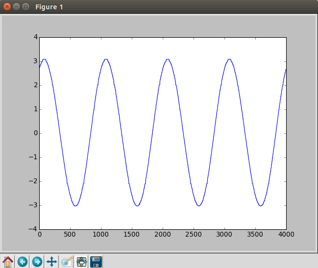
Figure : The circuit used for making the half-wave rectifier and studying it. A bipolar sinusoidal signal is input to a diode, and the output voltage is monitored. The 1uF capacitor is used to filter the output signal and make it more or less constant, but it has not been used while obtaining the data shown in the following image

We can observe that only the positive half of the signal passes through the diode. It can also be observed , that since this is not an ideal diode, the conducted portion has lost some amplitude. This loss is a consequence of the forward threshold voltage of the PN junction, and in case of this diode, it is around 0.6 Volts. This threshold voltage depends on the band structure of the diode , and in the next section we shall examine this voltage for various diodes.
Measurement of Current-Voltage Characteristics of diodes
In practice, diodes only start conducting in the forward direction after a certain threshold potential difference is present. This voltage, also known as the barrier potential, depends on the band gap of the diode, and we shall measure it to determine how the electrical properties affect the externally visible physical properties of the diode.

A programmable voltage output of the PSLab (PV1) will be increased in small steps starting from 0 Volts, and a voltmeter input (CH3) will be used to determine the point when the diode starts conducting. The presence of a known resistor between PV1 and CH3 acts as a current limiter, and also enables us to calculate the current flow using some elementary application of the Ohm’s law. I = (PV1-CH3)/1000 .
The following image shows I-V characteristics of various diodes ranging from Schottky to Light Emitting Diodes (LEDs).

It may be interesting to note that the frequency of the light emitted by LEDs is directly proportional to the threshold voltage. In case of the white LED, it is almost similar to the blue LED because white LEDs are composed of blue LEDs, and a phosphor coating that partially converts blue light to yellow. The combination results in white light.
Zener diodes
Zener diodes are a special variant of diodes that also conduct electricity in the the reverse direction once a certain threshold has been crossed. This threshold can be determined during the manufacturing process, and zener diodes with breakdown voltages such as 3.3V , 5.6V , 6.8V etc are commercially available.
In the following image, the I-V characteristics of a 3.3V zener diode have been measured with the PSLab . As can be observed, the diode starts to conduct small amounts of current from around 2V itself, but significant current flow is usually present once the rated voltage is achieved.
In the forward direction, the zener appears to behave as a regular diode.

Resources
- Introduction to P-N Junctions : http://www.electronics-tutorials.ws/diode/diode_3.html
- P-N junction theory : http://www.electronics-tutorials.ws/diode/diode_2.html
- Zener Diodes : https://en.wikipedia.org/wiki/Zener_diode
- Light Emitting diodes : http://www.electronics-tutorials.ws/diode/diode_8.html


 An example of a pulse sensor designed with just the voltmeter and a digital output of the PSLab.

You must be logged in to post a comment.