

Create a Distance Sensor using PSLab
PSLab device is a small lab which supports a ton of features. Among its many features, integrating a distance measuring sensor like HC SR04 sonar sensor into it is one of them. This blog post will bring out the basic concepts behind a sonar sensor available in the current market, how it measures distance and how it is implemented in the PSLab device.
A sonar sensor uses a sound wave with a very high frequency. These waves are called ultrasonic waves. They cannot be heard by the naked ear. Human ear can only hear frequencies from 20 Hz up to 20 kHz. Generally HC SR04 sensors use a wave with frequency as high as 40 kHz so this makes sense. The basic principal behind the sensor is the reflectance property of sound. Time is calculated from the transmission time up to the time receiving the reflected sound wave. Then using general moment equation S = ut; with the use of speed of sound, the distance can be measured.
 The figure shows a HC SR04 ultrasound sensor. They are quiet famous in the electronic field; especially among hobbyists in making simple robots and DIY projects. They can be easily configured to measure distance from the sensor up to 400 cm with a measuring angle of 15 degrees. This angular measurement comes into action with the fact that sound travels through a medium in a spherical nature. This sensor will not give accurate measurements when used for scenarios like measuring distance to very thin objects as they reflect sound poorly or there will not be any reflectance at all.

There are four pins in the HC SR04 sonar sensor. Corner pins in the two sides are for powering up the Sonar sensor. The two pins named ECHO and TRIG pins are the important pins in this context. When the TRIG pin (Trigger for short) is excited with a set of 8 square pulses at a rate of 40 kHz, the ECHO pin will reach to logic HIGH state which is the supply voltage (+5 V). When the transmitted sound wave is reflected back to the sensor, this high state of the ECHO pin will shift to logic LOW state. If a timer is turned on when the ECHO pin goes to logic HIGH state, we can measure how long it was taken for the sound beam to return to the sensor by turning off the timer when the ECHO pin goes to logic LOW state.
Having described the general implementation of a sonar sensor; a similar implementation is available in PSLab device. As mentioned earlier, TRIG pin requires a triggering pulse of 8 set of square waves at 40 kHz. This is achieved in PSLab using SQR pulse generating pins. The time is measured from the transmitting point until the receiving point to evaluate the distance. The real distance to the obstacle in front of the sensor can be calculated using following steps;
- Measure total round trip time of the sound beam. Take it as t
- Calculate the time taken for the beam to travel from sensor to the obstacle. It will be t/2
- Use motion equation S = ut to calculate the actual distance taking u = speed of sound in air. Substituting the time value calculated in step 2 to t, S will produce the distance
Resources:
- Feature image from: https://www.allaboutcircuits.com/projects/measure-distance-with-a-sonar-sensor-on-an-arduino/
- https://github.com/fossasia/pslab-python/blob/development/PSL/sciencelab.py#L3972
- https://github.com/fossasia/pslab-hardware
- HCSR04 – https://docs.google.com/document/d/1wtYUBkN9-VnlpjCtu8RyhacgyHh4LP7e0jOrTGatwrY/edit?usp=sharing


 Let’s take a look at this circuit. We can clearly see that there is a series combination of a resistor and a capacitor at A and a parallel combination of a resistor and a capacitor at B joining at the non-inverting pin of the OpAmp. The series combination of RC circuit is nothing but a high pass filter that allows only high frequency components to pass through. The parallel combination of RC circuit is a Low pass filter that allows only the low frequency components of a signal to pass through. Once these two are combined, a band pass filter is created allowing only a specific frequency component to pass through.
 Using practical values for R as 10k, C value can be approximated to 33nF. This oscillator is capable of generating a stable 500 Hz sinusoidal waveform. By changing the resistive and capacitive values of block A and B, we can generate a wide range of frequencies that are supported by the Op Amp because Op Amps have a limited bandwidth it can be functional inside.


 There is a huge drawback with this design. The above calculation is valid only if there is no load impedance is present at the output terminals.
 Unlike the previous model, this model ensures that the output voltage will be maintained constant across the output terminals within a range of supply voltage values.
 For a zener diode to maintain a constant voltage level across output terminals, there should be a minimum current flowing through the diode. If this current is not flowing in the zener, there won’t be a regulation. Assume there is a very low load impedance. Then the current supplied by the source will find an easier path to flow other than through the diode. This will affect the regulatory circuit and the desired voltage will not appear across the output terminals.
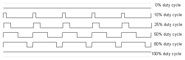
You must be logged in to post a comment.